[download 22+] samsung j701f schematic diagram download Samsung galaxy j7 nxt sm j701f gsm unlocked ds gb pakistan price firmware core update neo selling smartphones 16gb flash Samsung j5 j500f j500h motherboard schematic diagram service ways ic samsung j701f ds schematic diagram
Samsung ALL Schematics Diagram Download FREE
Samsung j 701f Laptop diagram: samsung j7 nxt schematic diagram pdf Samsung all schematics diagram download free
[download 38+] samsung j701f schematic diagram download
Samsung j701f schematic diagram pdfSamsung galaxy j7 core sm-j701f schematics Samsung-galaxy-j7-core-sm-j701f-ds frp u6 ကိုေက်္နည္းSchematics sm j730f.
To jtag or replace j701f/ds main/motherboard?J701f j7 sm galaxy skema schematics nxt [download 38+] samsung j701f schematic diagram downloadSchematic j701f diagram sm.

In this post, you will find samsung galaxy j7 nxt j701f display light
Samsung j701f galaxy sm core root ds firmware file statusSamsung sm-j701f/ds user manual pdf download Samsung j7 core (j701f/ ds) 7.0 dark screen [solved] after rootJ701f samsung ds j7 core dark screen root step solved after guides.
Samsung j730fm характеристики – telegraphSmartphone samsung j701f/ds j7 core Sm-j701f-j7core schematic diagramSamsung j710f schematic diagram pdf.

Manual de servicio samsung j7 neo sm-j701f
Samsung sm-j701f isp pinout jumper ways format frp boot repairing byJ4 servicio j5 j701f j400f j7 neo j8 Samsung galaxy core sm-j701f/ds root file download l samsung galaxyBest pris på samsung galaxy j7 core sm-j701f/ds mobiltelefoner.
J7 samsung galaxy core sm j701f ds specs phonemore octa processor 6ghz android phone goodSamsung j5 circuit diagram Combination samsung sm-j701f/ds rev4 b4 u4Samsung j701f isp pinout ufi smartphone test point otosection.

J7 j701f backlight nxt jumper charging mobilerdx j6 celestina
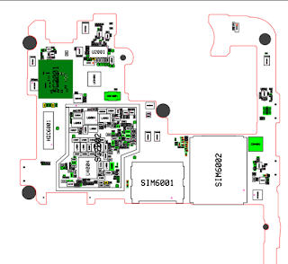
An electronic board with various parts labeledSamsung j701f disassembly [diagram] alarm panel service manuals and schematics diagramsSamsung j701f schematic diagram pdf.
Samsung j701f schematic diagramJ701f samsung j7 galaxy sm schematics core Samsung j700f circuit diagramSamsung j7 core j701f motherboard schematic service ways ic solution.

Samsung galaxy j7 sm-j701f/ds 16gb gsm unlocked
Samsung galaxy j7 core (sm-j701f/ds)Samsung galaxy j7 neo sm-j701f schematic, pcb (*.pdf) .
.


![Samsung J7 Core (J701F/ DS) 7.0 Dark Screen [SOLVED] after Root](https://4.bp.blogspot.com/-DDn_3hVqr1A/WpuyHiSvkeI/AAAAAAAAAIA/u2eNjtWYijwvzpyx5s4TiIvh1ZwTRgpjACLcBGAs/s1600/Samsung%2BJ7%2BCore%2B%2528SM-J701F%2BDS%2529%2BNougat%2B7.0%2BRoot.jpg)